

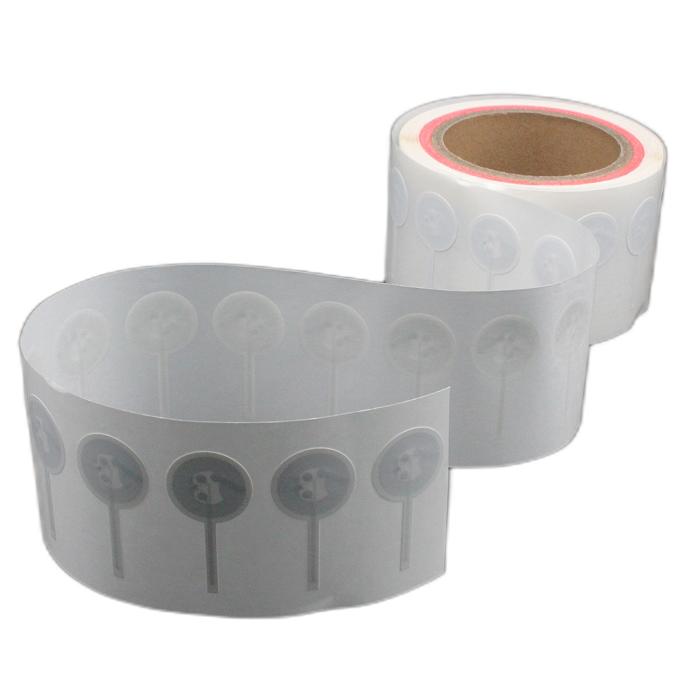
ODM RFID Inlay: Streamlining Custom Tag Design for Scalable Deployments
2026-05-10
Every RFID deployment starts with a critical choice: the inlay. Get it wrong, and you’re stuck with failed reads, delayed timelines, and costly redesigns. That’s why forward-thinking integrators are switching to ODM RFID inlays—a smarter path that combines custom precision with off-the-shelf speed. Unlike fully bespoke designs that drag on for months, ODM solutions from OSRFID let you tailor proven inlay platforms to your exact needs, slashing development cycles while ensuring performance at any scale. Imagine launching a supply chain pilot in weeks, not quarters, without sacrificing reliability. In this post, we’ll unpack how ODM RFID inlays bridge the gap between generic and custom, and why they’re the secret weapon for scalable, hassle-free deployments.
Rethinking Inlay Design: The ODM Advantage
The standard approach to inlay work often stumbles on a narrow path, where design ambition is quietly trimmed to fit the limits of in-house production. A team envisions a complex marquetry motif or a seamless metal-to-ceramic junction, but the tooling, material handling, or even the manual skill on hand says otherwise. This is where the rethink begins—not by scaling back the idea but by questioning who is best positioned to execute it. The real shift happens when you stop treating the inlay as a craft problem to be solved in isolation and start seeing it as a workflow challenge that benefits from outside perspective and purpose-built setup.
An ODM partner flips the entire dynamic. Instead of handing off a finished blueprint and hoping for a faithful copy, you bring a rough concept, a material palette, and a set of functional demands. The manufacturer then loops in their prototyping capacity, their material science know-how, and years of niche process experience to shape the inlay not just to the product but to the production line. The result is rarely a generic solution. It’s an inlay that fits the enclosure curves with fewer post-process adjustments, uses bonding techniques that speed up assembly, or introduces mixed materials in ways an internal team might never risk testing. What lands on your desk isn’t a sample that whispers “this is as good as we can get” but a repeatable part that quietly opens new design territory.
Customization Demystified: Tailoring Tags to Unique Environments
Every deployment landscape carries its own quirks—what works flawlessly in a staging server might crumble under the weight of a production setup. Customization isn’t about piling on options; it’s about surgically adapting tags to mirror the actual flow of data, the naming conventions your team already uses, and the quirks of your legacy systems. When tags reflect reality rather than a generic template, they stop being a maintenance headache and start acting as a seamless extension of your environment.
The real trick lies in understanding which layers need flexibility. A tag hierarchy that makes sense for a monolithic architecture often becomes a liability in a microservices setup. By letting teams define granular rules—like how to handle regional variations, department-specific identifiers, or fluctuating load patterns—you turn a static labeling system into a living map of your infrastructure. This approach sidesteps the common trap of forcing a one-size-fits-all logic onto a landscape that demands nuance.
Start small by pinpointing the three most unstable variables in your current setup. Maybe it’s inconsistent versioning across environments, or tags that keep colliding because of overlapping time zones. Build your customization around these pressure points first, then expand outward. The goal isn’t to create a perfect taxonomy overnight; it’s to craft a tagging strategy that bends where it needs to, so your team spends less time wrestling with labels and more time building momentum.
Production Efficiency: From Prototype to High-Volume Output
Moving from a hand-built prototype to mass production is rarely a straight line. Small design tweaks that seem harmless during R&D can cascade into major bottlenecks on the factory floor. Early cross-team collaboration—between engineers, manufacturing, and supply chain—helps catch these snags before they delay ramp-up. It’s not just about designing for function; it’s about designing for repeatability, tolerances, and the real-world quirks of assembly lines. When those conversations happen early, the shift from low-volume pilot runs to full-scale output becomes far less chaotic.
Process refinement is where efficiency gains really multiply. Instead of chasing perfect upfront plans, top-performing manufacturers rely on iterative improvements once production begins. They track yield rates, cycle times, and material flow relentlessly, then tweak workstations, tooling, or supplier specs based on actual data. Sometimes the biggest breakthroughs come from simply rearranging a cell layout or standardizing a frequently missed step. This mindset turns scaling into a continuous learning loop rather than a one-time handoff.
Technology plays a key role, but it’s not a silver bullet. Automated inspection systems, digital work instructions, and predictive maintenance tools can shave seconds off each unit and cut defect rates significantly. Yet the real edge comes from blending these tools with a culture that empowers line workers to flag issues and suggest fixes. When a company pairs smart automation with on-the-ground insight, it doesn’t just hit volume targets—it consistently delivers quality as output climbs. That balance is what separates a chaotic launch from a smooth, profitable scale-up.
Scalability Tactics for Enterprise-Wide RFID Implementations
When rolling out RFID across multiple facilities, the architecture must gracefully handle surges in tag reads without buckling. One practical method is to deploy edge processing units that filter and aggregate data locally before forwarding only meaningful events to central systems. This reduces bandwidth demands and decouples the core platform from raw reader noise, letting each site operate semi-autonomously even during network hiccups.
Database design plays an outsized role in maintaining performance as the volume of tagged items climbs into the billions. A time-series optimized storage layer, combined with strategic data partitioning by location or time window, keeps query latencies predictable. Rather than indexing every attribute, focus on the access patterns that matter for inventory reconciliation and asset tracking, and let less critical detail reside in colder, cost-efficient archives.
Middleware scalability often hinges on how well the system manages reader coordination. Instead of a naïve round-robin scheme, intelligent scheduling based on antenna beam overlap and tag population density prevents radio collisions and phantom reads. Pair this with auto-scaling message brokers that expand during peak shipping hours, and the RFID backbone remains both responsive and cost-effective as the business grows.
Balancing Durability and Performance in Challenging Conditions
In demanding environments where equipment faces constant vibration, extreme temperatures, or corrosive substances, the typical design focus tends to lean heavily toward ruggedness. However, overbuilding can inadvertently add weight and restrict functionality, creating a new set of performance hurdles. The real expertise lies in choosing materials and structural geometries that stand up to punishment without bloating the system's footprint or slowing its response times. For instance, innovations in alloy composition have allowed for thinner, lighter enclosures that still dissipate heat effectively while resisting impact. Engineers are learning that durability isn’t just about brute strength—it’s about intelligent compromise that keeps the device operating at full potential even when conditions turn foul.
One underappreciated aspect is the role of buffering and damping at the interface level. Rather than simply hardening every component, strategic use of elastomeric mounts or conformal coatings can isolate sensitive electronics from the worst of the stress while preserving signal integrity and connectivity. This approach often pays dividends in fluid systems or high-pressure settings, where rigid assemblies can crack or micro-fracture over time. By letting the structure flex imperceptibly, these solutions forestall fatigue while maintaining the tight tolerances required for speed and precision. It’s a mindset shift: viewing durability not as a shield but as a dynamic balance that keeps the machine running smoothly across a wide range of inputs.
Field data consistently shows that designs prioritizing this equilibrium between toughness and agility extend service intervals and reduce unplanned downtime. Teams that incorporate real-time monitoring—tracking strain, temperature, and wear patterns—can fine-tune this balance continuously rather than relying on static safety margins. The result is equipment that not only survives but thrives where others falter, delivering consistent output without the weight penalty that drags on efficiency. In the end, the hallmark of engineering excellence in harsh conditions is not how much punishment a system can take, but how effortlessly it performs while taking it.
Future Trends: The Evolution of Smart Inlay Architectures
The next wave of smart inlays will be defined not by incremental improvements but by a radical rethinking of the substrate itself. Traditional rigid carriers are giving way to ultra-thin, flexible polymers that can conform to curved surfaces, enabling seamless integration into wearable textiles, medical patches, and even temporary tattoos. These materials are being engineered at the molecular level to combine structural resilience with high-fidelity signal propagation, allowing antennas and sensors to be printed directly onto the inlay using conductive inks. The result is a blurring of the boundary between the object and the electronics, where the inlay becomes an inseparable part of the product’s physical identity rather than an added component.
Energy autonomy is emerging as a cornerstone of future architectures. Instead of relying on external readers or batteries, next-generation inlays will harvest ambient energy from radio waves, body heat, or micro-motion. This shift demands a new design logic: the inlay must be optimized as a multi-functional energy and data node, with power management circuitry embedded at the chip level. Coupled with advances in ultra-low-power microcontrollers, these inlays will sustain continuous sensing and sporadic communication for years without maintenance. The architecture becomes a self-sustaining ecosystem, opening doors to applications like infrastructure monitoring where physical access is impractical.
Perhaps the most disruptive change will come from the convergence of smart inlays with edge AI. Rather than transmitting raw data, the inlay itself will pre-process information, making decisions locally before engaging with a network. This requires a co-design of silicon and antenna geometry tailored to specific inference tasks, such as anomaly detection or gesture recognition. By pushing intelligence to the physical edge, these architectures drastically reduce latency and bandwidth demands while enhancing privacy. The inlay evolves from a passive identifier into an active, context-aware agent embedded in the fabric of everyday life.
FAQ
An ODM RFID inlay is a custom-engineered tag where the manufacturer designs the antenna, chip bonding, and substrate specifically for your application, rather than picking a generic design from a catalog. The key difference lies in performance tuning—ODM inlays are optimized for your exact materials, read range, and environmental conditions, so you get better reliability and consistency in the field.
Companies often turn to ODM when off-the-shelf tags fall short of unique requirements—such as needing to work on metal surfaces, curved items, or within dense packaging. ODM design allows you to tailor the tag to the product’s form factor and reading environment, eliminating the trial-and-error of testing dozens of generic tags. It also gives you control over performance metrics, so you’re not settling for ‘good enough.’
It removes the back-and-forth guesswork. A reputable ODM partner starts with a deep dive into your use case—measuring dielectric properties, analyzing reading angles, and simulating antenna layouts—before building physical samples. This data-driven approach compresses design iterations and avoids costly re-spins. Once validated, the same team handles volume manufacturing, so the transition from prototype to full-scale rollouts is seamless.
Absolutely. Because the design is purpose-built and thoroughly tested on your actual products, every inlay that comes off the production line performs identically in your environment. The manufacturing process is tightly controlled to maintain tolerances, and the inlay can be delivered in high volumes with batch-to-batch repeatability, which is critical when you’re tagging millions of items across multiple locations.
They shine where standard tags struggle: item-level tracking of metallic tools, embedded sensors in aircraft parts, laundry tags that survive industrial washing, pharmaceutical vials with small form factors, or smart packaging that requires a specific read zone for automated kiosks. In short, any scenario where the asset’s material, shape, or usage pattern kills generic tag performance.
The substrate and antenna are finely matched to the product’s surface. For instance, a flexible inlay with a meandered dipole might be designed to detune around liquids, while a rigid inlay with a patch antenna focuses energy forward through thick plastic. The geometry controls impedance and radiation pattern, so the tag can be tuned for near-field reads at a point-of-sale or far-field scans in a warehouse aisle.
The chip dictates memory size, sensitivity, and security features, so it’s chosen based on the data payload and read requirements. For large-scale rollouts, you might opt for a chip with a fast anti-collision algorithm to handle dense tag populations, or one with extended EPC memory to store unique identifiers beyond a simple serial number. ODM experts match the chip to the antenna and the system’s reader infrastructure to ensure reliable singulation at speed.
Start by assessing the complexity of your assets and the real-world read rates you need. If you’ve already tried sample kits and faced inconsistent results, or if your project demands tags that blend invisibly into a product’s design, an ODM approach is worth exploring. Look for a partner that offers RF simulation, rapid prototyping, and in-house manufacturing—this reduces risk and speeds up time-to-deployment. A pilot run on a small portion of your use case will quickly prove the value.
Conclusion
The shift toward original design manufacturing (ODM) for RFID inlays fundamentally rethinks how custom tags are conceived, moving beyond one-size-fits-all approaches. By embedding customization early in the design phase, ODMs enable tags tailored precisely to unique environments—whether that means optimizing antenna geometry for dense metal surroundings or selecting substrates that survive chemical washdowns. This early-stage collaboration shortens the feedback loop between concept and prototype, letting enterprises iterate rapidly without the usual back-and-forth of traditional procurement. The result is a purpose-built inlay that balances durability and performance from the outset, sidestepping the compromises common with pre-fabricated chips.
Production efficiency scales naturally once the design is mature. With ODM workflows, the transition from pilot to high-volume output avoids the bottlenecks of retooling or supplier handoffs, keeping lines moving during enterprise-wide rollouts. Scalability tactics such as panel-level manufacturing and in-line testing are baked into the process from day one, ensuring consistent quality whether you need ten thousand tags or ten million. Looking ahead, the evolution of smart inlay architectures—integrating sensing, encryption, or energy harvesting—will lean heavily on ODM agility. As demands for batch-level traceability and ruggedized form factors intensify, the ODM model strips out complexity, delivering streamlined tag solutions that keep pace with ever-changing deployment landscapes.
Contact Us
Contact Person: Esme Mo
Email: [email protected]
Tel/WhatsApp: 0086 191 2931 7837
Website: https://www.osrfidglobal.com/